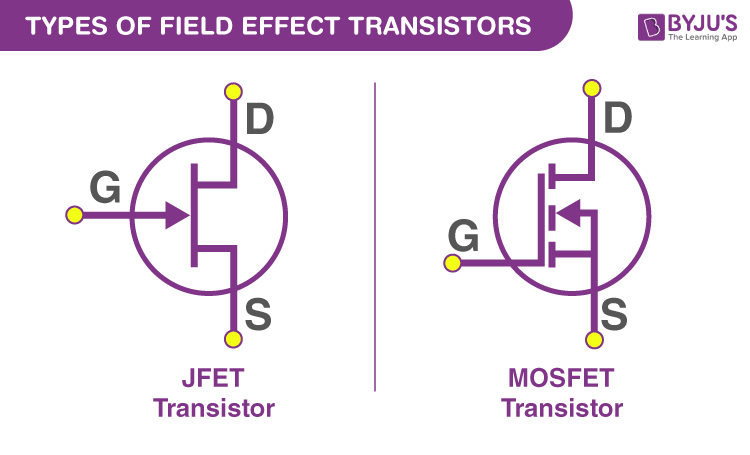
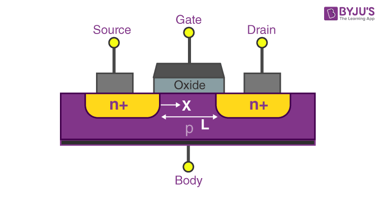
The FET transistor (field-effect transistor) controls the form and thus the conductivity of the charge carrier in a semiconductor through an electric field. As they undergo an operation of a single-carrier type these FET transistors are also called unipolar transistors. All the forms of FET have high input impedance. The input current regulates the conductivity of a non-FET transistor and thus is low in the input impedance. A field-effect transistor’s terminals have applied a voltage through which conductivity is regulated. The voltage that was applied to the gate creates an electric field in the device which causes repulsion and attraction to charges that are carried amid the two terminals. The conductivity is also affected due to the density of those charge carriers.
History of FET Transistor
Julius Edgar filed the first patent for a field-effect transistor in 1926 and then Oskar Heil too did the same in 1934. The junction gate field-effect transistor was created when William Shockley of the Bell Labs observed and elucidated the transistor effect in 1947. More developments were made to the device in later years of the 20th century.
Types of FETs:
There are two types of Field Effect Transistors:
- Junction Field Effect Transistor (JFET)
- Metal oxide semiconductor Field Effect Transistor (MOSFET)

| Similar Reading: |
| MOSFET |
| JFET |
Essential Information concerning FETs

There are two types of FET’s one will be in which the current is taken primarily by majority carriers and thus are majority charge carrier devices. The other will be where the current flow is primarily due to the minority carriers and thus are called minority charge carrier devices. The electrons flow to the drain from the source through active channels in the device. The ohmic contacts connect both the terminal conductors to the semiconductors. The source terminal and the gate have a potential between them and the conductivity of the channel is a function of it.
There are three terminals when it comes to FET:
- IS is the term used for the current that enters through our first terminal that is the source.
- ID is the term used for the current that leaves the channel through the drain (D). The voltage between drain to source is VDS .
- The channels conductivity is modulated by the gate (G). ID can be controlled by applying a voltage at G.
The functions of the above-mentioned gates explain their names. The working of these gates is similar to a gate in real life as in the terminal controls when they open and when they close. The gate can either choose to permit the passage of electrons or stop it.
Learn further about MOSFET and JFET transistors with engaging videos by downloading BYJU’S Learning App.


Comments